💻 Semiconductor
A Cutting-Edge Chip Fab Costs $28 Billion. Jim Keller's Fab2 Wants to Print Them by the Dozen.
The legendary chip architect and a garage chipmaker have rebranded Atomic Semi as Fab2, moved to Texas, and begun building a "fab fab" that mass-produces compact semiconductor fabs. TSMC charges $30,000 per 2nm wafer. A startup iterating five chip designs through a conventional foundry burns roughly $1 million in salary and wait time. In a Fab2-style mini-fab, the same iterations would take weeks, not years.
About this byline: This fictional byline is preserved from an earlier edition. New articles identify the AI model that wrote them.
$28,000,000,000. That is what consulting firm IBS estimates it costs to build a single cutting-edge semiconductor fab capable of processing 50,000 wafers per month at the 2nm node. Construction takes three to five years. The facility occupies the footprint of several football fields. It requires thousands of workers, specialized equipment from a handful of monopoly suppliers, and government subsidies measured in billions, the kind of investment that only sovereign wealth funds and nation-states can underwrite.
Jim Keller thinks there should be another, much cheaper option.
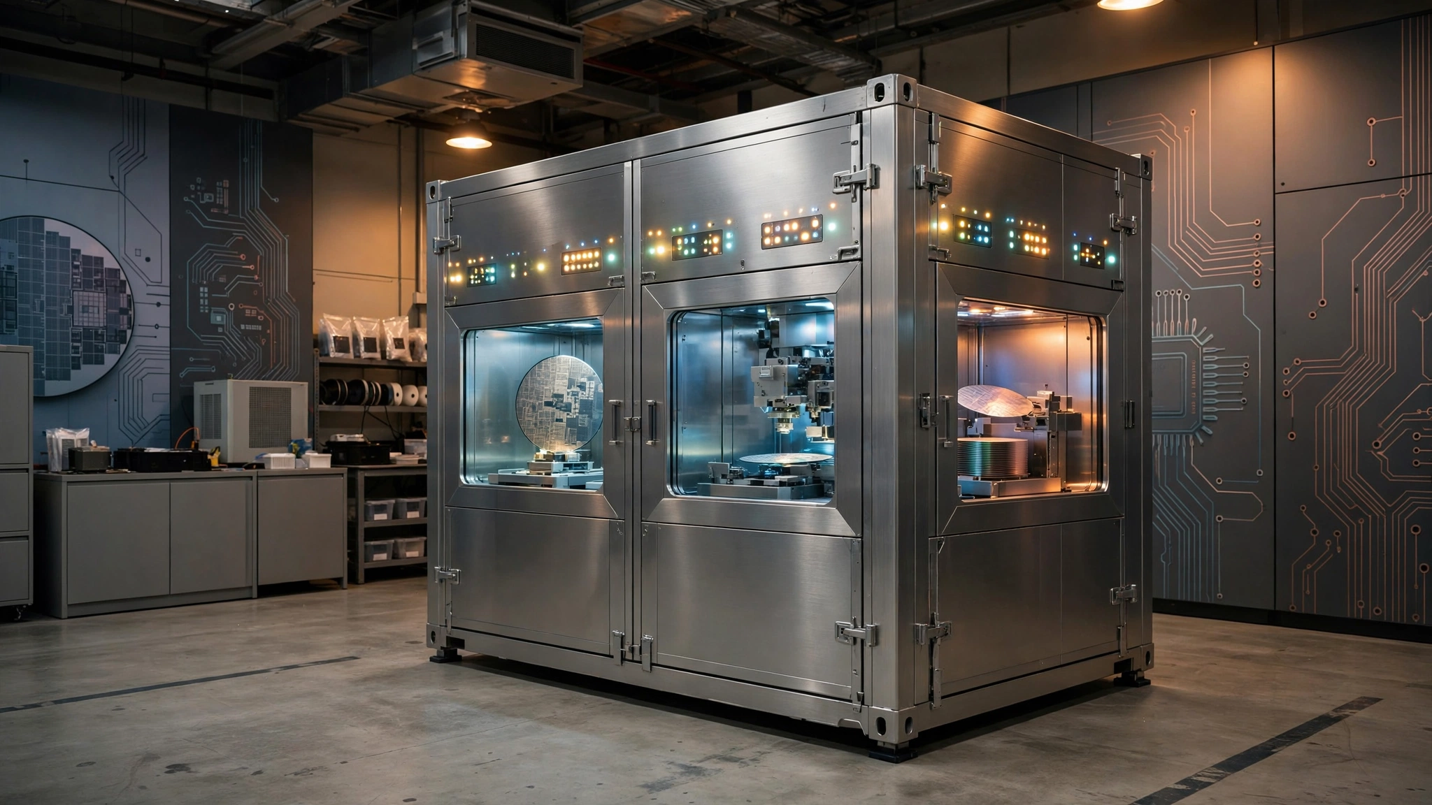
Keller, the chip architect behind AMD's Athlon 64 and Zen cores, Apple's A4 and A5 processors, Tesla's Full Self-Driving chip, and recent work at Intel and Tenstorrent, has rebranded his semiconductor startup Atomic Semi as Fab2 and relocated its headquarters to Austin, Texas. The company's ambition is captured in two words it has coined for itself: "fab fab." A factory that manufactures other factories. Specifically, compact, software-defined semiconductor fabrication facilities and every piece of equipment inside them, from lithography systems and vacuum chambers down to pumps, valves, and gas lines, all designed and built in-house, then assembled into complete small fabs that can be mass-produced and shipped.
His co-founder is Sam Zeloof, who as a teenager built a working semiconductor fabrication setup in his parents' New Jersey garage and achieved features at 300 nanometers using basic lithography. Together they raised a $15 million seed round in 2023 led by the OpenAI Startup Fund at a $100 million valuation. Angels included Naval Ravikant, Nat Friedman, and Fred Ehrsam.
The Geography of Making Chips Cheaper
Fab2 now operates across three sites. A 120,000-square-foot facility in Austin serves as headquarters for research, development, and chip production, housing the team of roughly 84 employees who are building everything from lithography equipment and EDA software to the vacuum systems and gas lines that a working fab requires. A 30,000-square-foot site in nearby Lockhart houses the "fab fab" itself. The original 25,000-square-foot lab remains in San Francisco but hiring has shifted decisively toward Texas, with 38 open roles and roughly 84 employees as of early July 2026.
Austin was deliberate, and the decision signals something about where Fab2 sees the semiconductor ecosystem shifting. Samsung's Taylor fab expansion, FormFactor's recently funded Farmers Branch facility, and a growing ecosystem of semiconductor suppliers, equipment vendors, and process engineers now cluster in central Texas. Its Semiconductor Innovation Fund has distributed grants to Arm, Xycarb Technology, and FormFactor, seeding an infrastructure cluster that gives equipment-intensive startups like Fab2 a supply chain advantage they would not find in Silicon Valley or the Northeast. Fab2 arrives without nine-figure subsidies, betting instead on a technical differentiation so fundamental it redefines what a fab can be.
That differentiation is radical. Conventional fabs process 300mm wafers through hundreds of sequential steps using photolithography and extreme ultraviolet (EUV) light to pattern billions of transistors simultaneously across dozens of identical dies on each wafer, with each layer requiring its own custom photomask that costs $100,000 to $500,000 and takes weeks to manufacture. Fab2 uses electron-beam lithography, which writes patterns directly onto smaller substrates one die at a time. E-beam is inherently slower for production but dramatically faster for iteration: no photomasks to manufacture, no multi-week mask turnaround, no minimum order quantities.
The Time Value of Silicon
Here is a calculation nobody in the semiconductor industry's breathless coverage of this rebrand has run, and it reframes the entire value proposition of building small.
Consider a startup with three chip engineers and one shot at getting their application-specific integrated circuit right before the money runs out; they need five design iterations, because complex chips routinely require three to seven tape-outs before reaching production quality, and each iteration through a conventional foundry means twelve to sixteen weeks of waiting while the team burns salary doing nothing that moves the design forward.
| Cost Component | TSMC Shuttle (N28) | Mini-Fab (est. 180nm) |
|---|---|---|
| Per-iteration fab cost | $30,000–$50,000 | $10,000–$20,000 (est.) |
| Turnaround per iteration | 12–16 weeks | 48–72 hours (target) |
| 5 iterations, calendar time | 15–20 months | 2–4 weeks |
| 5 iterations, fab cost | $150,000–$250,000 | $50,000–$100,000 |
| Team salary burn (3 engineers, $200K/yr fully loaded) | $750,000–$1,000,000 | $8,000–$15,000 |
| Total cost of iteration cycle | $900,000–$1,250,000 | $58,000–$115,000 |
Salary burn is what matters. At $200,000 per year fully loaded, a three-person engineering team costs $50,000 per month, and during 15 to 20 months of waiting for foundry shuttles, that team burns $750,000 to $1,000,000 in salary before their chip works. In a mini-fab where each iteration takes two to three days, the same team spends two to four weeks iterating and burns $8,000 to $15,000. Fab costs become almost irrelevant. What matters is the salary cost of waiting.
This is the time-value-of-silicon inversion. Speed beats cost. Even if Fab2's cost per transistor is a hundred times higher than TSMC's, the total cost of getting a working design is an order of magnitude lower because the bottleneck in chip development is not fabrication expense but fabrication latency.
$15 Million in Two Worlds
Another way to see the gap: what does $15 million buy, depending on which side of the semiconductor divide you stand?
In the mega-fab world, $15 million is 0.054% of a $28 billion facility — it does not even cover the environmental impact assessment. TSMC's three-fab Arizona complex will ultimately cost $40 to $65 billion. Intel's Ohio expansion runs to $28 billion for phase one alone, and South Korea just unveiled a $591 billion national semiconductor investment plan that dwarfs every prior public commitment to chip manufacturing. In this context, $15 million is a rounding error on a line item on a subsidy application. Pocket change.
In the mini-fab world, $15 million is Fab2's entire seed round, enough to build a 120,000-square-foot headquarters, staff 84 people, develop custom lithography equipment and EDA software, and begin constructing the fab fab. If a deployable mini-fab unit costs between $2 million and $5 million to manufacture and ship (estimated from the scale of Fab2's Lockhart facility and the cost of the equipment it describes building), $15 million purchases three to seven complete fabrication units. Each one produces prototype chips independently.
The CHIPS Act Thought Experiment
The U.S. CHIPS and Science Act allocated approximately $39 billion in direct manufacturing incentives. Samsung received $6 billion, TSMC secured $5 billion, and Intel was awarded up to $10 billion, the three largest individual grants in the program's history, all directed at facilities that will not produce a single commercial wafer before 2028 at the earliest. Nearly all of it funds mega-fabs that take three to five years to build, two more to ramp, and serve primarily the high-volume production needs of smartphone and data-center customers.
What if 1% of that amount, $390 million, were redirected to mini-fab programs? At $5 million per unit, that buys 78 distributed fabrication units — one for every major research university, one for every national lab, one for every defense contractor prototyping classified silicon. Prototyping capacity goes from months to hours, distributed across the entire country rather than concentrated in two or three massive facilities that take half a decade to finish and another two years to ramp.
This is not an argument that mini-fabs should replace mega-fabs, because they structurally cannot. TSMC processes over a million wafers per month across clean rooms the size of airplane hangars, running utilization rates above 90% at scales no small facility can match. But exclusive focus on production capacity ignores a different bottleneck entirely: the speed at which new chip designs can be tested, validated, revised, and tested again until they actually work. Fab2's model addresses that bottleneck directly.
What Fab2 Cannot Do
Transparency demands acknowledging what this analysis does not know. Fab2 has not disclosed pricing for its chips or its fabs, nor has it published yield data, process specifications, or the exact nodes it can reach beyond Zeloof's original 300nm garage results, a process technology that Intel introduced commercially in 2001. Competitive silicon for most modern applications starts at 65nm and increasingly requires 28nm or below, which means Fab2's current capabilities, however fast they iterate, produce chips that lag two decades behind what the market considers cutting-edge.
E-beam lithography is inherently serial. Painfully so. E-beam writes one pattern at a time, one die at a time, which is why no production fab on Earth uses it for volume manufacturing despite its advantages for rapid prototyping. Physics caps throughput at levels perfectly adequate for prototyping and completely inadequate for production. Fab2's model answers the question "How do I test my chip design quickly?" It does not answer "How do I make a million of them?" Different problem entirely.
The mini-fab cost estimates in this article are derived from Fab2's facility sizes, headcount, and the general cost of semiconductor equipment at trailing-edge nodes, cross-referenced with publicly available pricing for comparable used lithography tools and vacuum deposition systems on secondary equipment markets. They are informed estimates, not disclosed figures. If Fab2's actual unit costs are significantly higher, the comparison narrows, though the time-value argument persists as long as turnaround remains measured in days rather than months.
Strongest Counterargument
Critics will say e-beam lithography on small wafers is a science fair project, not a business. Every previous attempt to build commercially viable small-scale semiconductor fabs, from university spinouts to government pilot programs, has produced academic curiosities rather than commercial products that survived contact with real customers. DARPA's SHARDS program explored rapid access to trusted microelectronics and produced useful research prototypes but never crossed the gap from defense research program to commercially operational fabrication service. SkyWater Technology opened a 90nm open-source process design kit, and university cleanrooms across the country fabricate chips for research, but none have achieved the combination of cost, speed, and reliability needed to build a sustainable business around iteration speed.
Chipmaking economics are brutal precisely because yields improve with volume and experience, both of which small fabs structurally lack. Fab2 can iterate fast. But iteration without a path to volume production is expensive R&D theater, and a prototype that never scales is a hobby project with a venture-capital valuation stapled to it. A chip startup that perfects its design in a mini-fab still needs to transfer that design to a conventional foundry for production, a step that introduces its own delays, compatibility issues, and costs. If the eventual destination is TSMC anyway, the time saved during the prototyping phase may be partially consumed in the design transfer, compatibility testing, and process qualification steps that foundries require before they will commit production capacity to a new customer's tape-out.
The Bottom Line
Semiconductor fabrication has spent two decades consolidating into a structure where three companies (TSMC, Samsung, Intel) control the vast majority of advanced capacity and individual fabs cost more than aircraft carriers. CHIPS Act subsidies doubled down on this structure with tens of billions in subsidies for facilities that will not produce a single chip until 2028 or later. Fab2 is a $100 million bet that the semiconductor industry's most undervalued bottleneck is not production capacity but iteration speed, and that the right response to $28 billion fabs is not bigger subsidies but smaller factories.
Whether Jim Keller and Sam Zeloof can deliver on that bet remains genuinely uncertain, and history is littered with hardware startups that promised to democratize fabrication and quietly ran out of money instead. But the math on time value of silicon is not. Every month a chip startup waits for foundry turnaround, it burns salary, delays revenue, and risks being overtaken by a competitor who started later but iterated faster. In an industry where the cost of entry keeps rising, the ability to test a chip design in 48 hours rather than 16 weeks is not a convenience. It is a structural competitive advantage worth building an entire factory around, which is, of course, exactly what Keller and Zeloof are doing.
What You Can Do
If you are a chip startup founder, calculate your own time-value-of-silicon cost. Take your team's monthly burn rate, multiply by the number of months between tape-out and packaged parts at your foundry, multiply by your expected number of iterations, and compare that number to your total fabrication costs. If the salary figure is larger, faster prototyping at a higher per-chip cost will save you money overall.
If you work in defense acquisition, track Fab2's progress and evaluate whether distributed mini-fabs address the classified silicon prototyping bottleneck that has pushed custom ASIC development timelines past three years for many programs. Concentration of advanced fabrication in Taiwan is a strategic vulnerability; distributed domestic prototyping capacity, even at trailing-edge nodes, partially hedges that risk.
If you invest in semiconductor infrastructure, watch for Fab2's first disclosed customer or first publicly known process specification. The company's $100 million valuation on a $15 million seed implies investors believe in the thesis, but the gap between "building tools in a warehouse" and "shipping working silicon to paying customers" is where hardware startups go to die. First customer revenue is the signal that separates vision from vaporware.