The U.S. Spent $52 Billion to Reshore Chips. Here's the Report Card.
TSMC Arizona is shipping 4nm chips to Apple and Nvidia at less than 10% cost premium over Taiwan. Samsung's $17 billion Texas fab is 91.8% built with zero confirmed customers. Intel's first chip on its own 18A process debuted at CES 2026. Two years into the CHIPS and Science Act, we graded every major recipient on what they promised versus what they delivered.
In August 2022, President Biden signed the CHIPS and Science Act into law, committing $52.7 billion in federal funding to rebuild domestic semiconductor manufacturing. The pitch was straightforward: the United States manufactured 37% of the world's chips in 1990, produced 12% by 2022, and made exactly 0% of the most advanced logic chips. That last number was the one that kept Pentagon planners awake.
Two and a half years later, the first American-made advanced chips are shipping. $450 billion in private investment has been pledged. Over 50,000 construction workers are building fabs across four states. But the results are wildly uneven. One recipient is ahead of schedule. One built a $17 billion shell with nothing inside it. One is trying to reinvent itself while burning billions per quarter. Here is the scorecard.
The Cost Myth That Won't Die
Before grading anyone, we need to kill the biggest misconception in the semiconductor reshoring debate: the idea that making chips in America costs 50% to 150% more than making them in Taiwan.
TSMC founder Morris Chang said in 2022 that building a fab in the U.S. would cost 150% more than Taiwan. Pundits ran with it. Some stretched it further. A Nikkei Asia analysis suggested costs could double. The number became dogma among reshoring skeptics.
It was wrong. Or more precisely, it was right about the wrong thing. Chang was talking about building a first fab with an untrained workforce. He was not talking about the per-wafer cost of running it.
TechInsights' Strategic Cost and Price Model, developed by analyst Scotten Jones and used by foundry customers worldwide to audit wafer pricing, ran the actual numbers. Their finding: it costs TSMC less than 10% more to process a 300mm wafer in Arizona than the same wafer in Taiwan.
Why? Plain math. Most people assume the cost gap comes from labor. American fab workers earn roughly 200% more than their Taiwanese counterparts. That sounds devastating until you realize that labor accounts for less than 2% of total wafer processing costs. Modern fabs are so automated that the humans are almost a rounding error.
Equipment is the dominant cost driver, consuming well over two-thirds of the per-wafer bill. An ASML EUV lithography system costs $380 million whether it ships to Tainan or Phoenix. Applied Materials etch tools, Lam Research deposition chambers, KLA inspection systems: same price, same throughput, same amortization schedule. When 67%+ of your cost base is globally uniform, the geography premium shrinks to single digits.
AMD CEO Lisa Su provided a second data point during a 2025 earnings call, confirming that chips produced at TSMC's Arizona fabs cost 5-20% more than Taiwan equivalents. The higher end of her range includes ramp-up inefficiencies that will shrink as the fab matures. The lower end aligns with TechInsights.
The Scorecard
| Recipient | CHIPS Award | Total Pledged | Status (March 2026) | Grade |
|---|---|---|---|---|
| TSMC | $6.6B | $65B | Shipping 4nm. 3nm equip install Q3 2026. | A |
| Intel | $8.5B | $100B | 18A debuted CES 2026. Foundry losses ongoing. | B− |
| Samsung | $4.7B | $37B | Taylor fab 91.8% built. Zero customers. | D |
| Micron | $6.1B | $100B (20yr) | Record revenue. NY megafab in planning. | B+ |
| GlobalFoundries | $1.5B | $11.6B | Expanding mature nodes. Strategic but limited. | C+ |
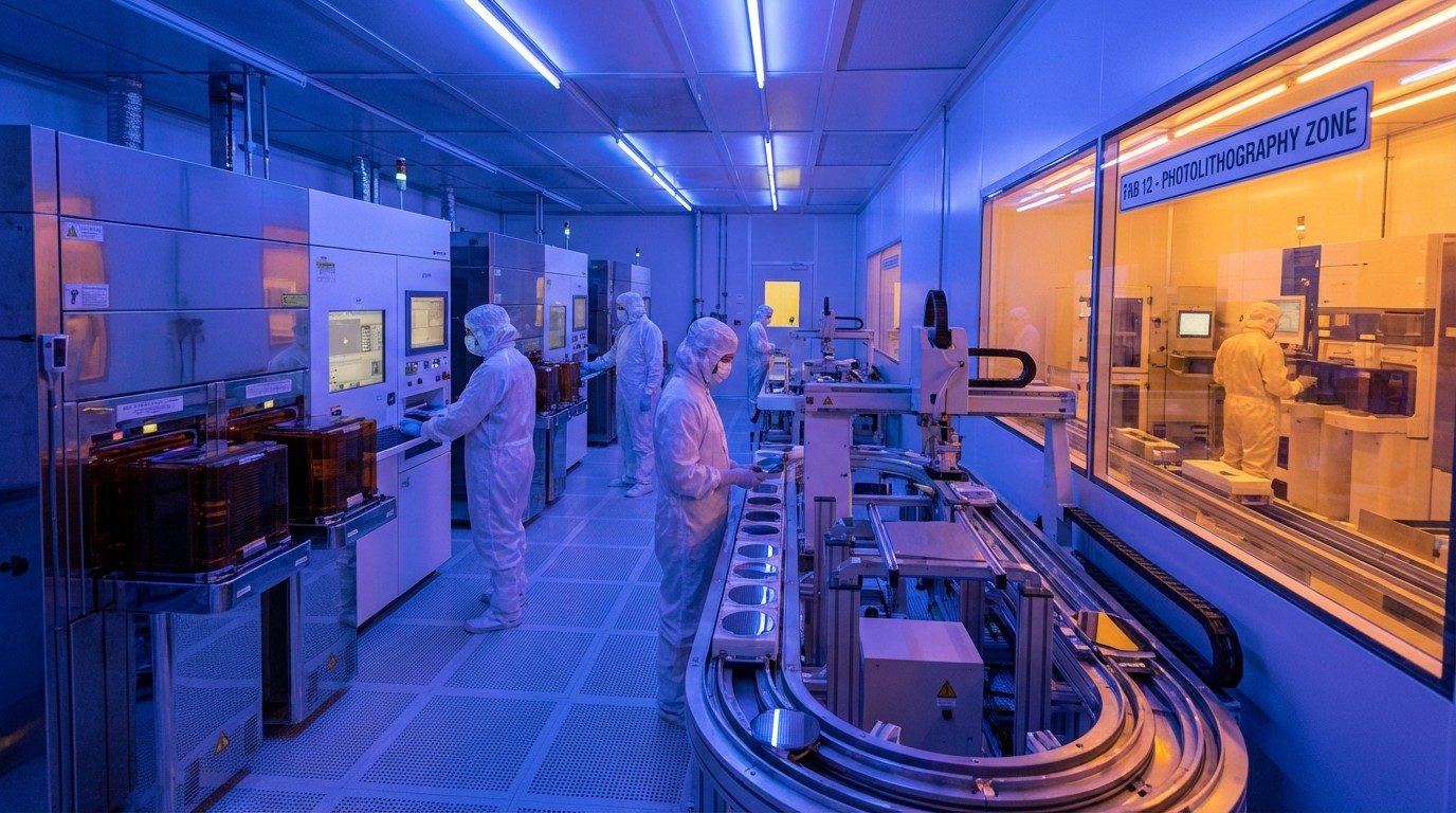
TSMC Arizona: The A Student
TSMC's first Arizona fab began producing 4nm chips in late 2024 and has since delivered wafers to Apple, Nvidia, and AMD. Those are not test runs. Those are production silicon going into commercial products. For context, 4nm is the process node powering the A17 Pro in the iPhone 15 Pro and Nvidia's data center GPUs.
TSMC's second Arizona fab is ahead of schedule. Construction started in April 2025, and 3nm equipment installation begins in Q3 2026, targeting volume production in 2027. A third fab is planned for 2nm and A16 nodes. Total investment across all three: $65 billion on 1,100 acres.
The catch: every chip made in Arizona still has to be shipped back to Taiwan for advanced packaging. TSMC's CoWoS (Chip-on-Wafer-on-Substrate) packaging, which stacks chiplets into the complex modules that Nvidia and Apple require, happens exclusively in Taiwanese facilities. The first U.S. advanced packaging plant won't break ground until Q3 2026. Until it's operational, "made in America" has an asterisk.
TSMC acknowledged during its July 2025 earnings call that overseas fabs dilute gross margins by 2-3%, rising potentially to 3-4% long-term. The company's response: raise prices. Starting in 2026, advanced nodes below 5nm get a 5-10% price increase globally, with U.S.-fabricated wafers carrying an additional premium. Current 3nm wafers run approximately $20,000 each. The upcoming 2nm node will exceed $30,000 per wafer, a 50%+ jump.
Samsung Taylor: The $17 Billion Warning
Samsung's Taylor, Texas fab tells a different story entirely. The company committed $17 billion and secured up to $4.7 billion in CHIPS Act grants. As of March 2025, the physical structure was 91.8% complete. The problem: no chip production equipment has been installed because Samsung has no confirmed customers.
When Samsung planned the Taylor fab in 2021-2022, its 4nm process was competitive. By the time the building was nearly finished, customers wanted 2nm. The technology shifted underneath the project. Retrofitting a fab designed for one process node to accommodate another is neither fast nor cheap.
Samsung's numbers tell a familiar semiconductor story. In Q1 2025, TrendForce pegged Samsung Foundry's global market share at 7.7%. TSMC held 67.6%. That gap is not just about scale; it reflects yield rates. Samsung's advanced-node yields have persistently underperformed TSMC's, and in the foundry business, yield is what converts a factory into a revenue generator. A beautiful fab with mediocre yields is an expensive building.
The Taylor fab was originally slated for production in 2024, then 2025, now 2026 at the earliest. Analyst Joanne Chiao of TrendForce told Nikkei Asia: "Samsung faced unstable yields and lost customer orders. Although yields have improved, restrictions on chip exports to China and lack of U.S. demand keep capacity underutilized."
Intel: The Hail Mary on 18A
Intel received the largest CHIPS Act award: $8.5 billion toward a $100 billion investment plan spanning fabs in Arizona, Ohio, New Mexico, and Oregon. The strategic bet: Intel could leapfrog TSMC by deploying its 18A process node, which uses both gate-all-around transistors and backside power delivery simultaneously.
At CES 2026, Intel debuted Panther Lake, the Core Ultra Series 3 processor and the first product built on 18A. That is a meaningful technical milestone. Intel is the only company attempting to run an advanced foundry while simultaneously being its own biggest customer, and 18A is the node that determines whether that dual strategy survives.
But the financials are brutal. Intel's foundry division has reported billions in operating losses. The company has announced layoffs, paused some construction, and restructured its foundry operation into a more independent subsidiary. External foundry customers remain scarce. Microsoft reportedly tapeout a test chip on 18A, but volume orders from outside Intel remain the missing proof point.
The B- grade reflects the tension between genuine technical progress and persistent commercial uncertainty. Intel is attempting something no company has done in the modern era: build a world-class contract foundry from scratch while competing with TSMC's 40-year head start. If 18A yields are competitive, the grade goes up fast. If they're not, the entire $100 billion plan unravels.
Micron and GlobalFoundries: The Supporting Cast
Micron's $6.1 billion CHIPS award supports a $100 billion, 20-year investment in memory fabrication, anchored by a planned megafab in Clay, New York. Micron reported record revenue in Q2 FY2026, driven by HBM (High Bandwidth Memory) demand for AI accelerators. Memory is a different game than logic: the U.S. has more existing capability, and Micron faces less direct competition from TSMC. Grade: B+.
GlobalFoundries received $1.5 billion for its $11.6 billion expansion of mature-node production in New York and Vermont. These are the 14nm-and-above chips that power cars, industrial equipment, and defense systems. Strategically important, but these aren't the leading-edge chips that triggered the CHIPS Act in the first place. Grade: C+.
Running the Numbers: What $52.7 Billion Bought
The CHIPS Act's leverage ratio is its strongest metric. Every $1 of public money has attracted roughly $8 in private commitments, producing over $450 billion in announced investments. That 8:1 ratio outperforms most federal subsidy programs.
The job creation numbers are large: 50,000+ construction jobs already active, with 40,000 direct manufacturing jobs expected once fabs reach full operation. Arizona, Ohio, Texas, and New York are the primary beneficiaries. TSMC's Arizona operations alone are projected to generate $100 billion+ in economic impact for the state.
The strategic metrics move more slowly. U.S. share of global chip production was 12% in 2022 and targets 20% by 2030. U.S. share of advanced logic nodes was 0% and targets 28% by 2030. Both are aspirational. TSMC Arizona shipping 4nm wafers means the advanced-node number is no longer zero, but reaching 28% requires Samsung, Intel, and future TSMC fabs to all deliver on schedule. Based on current trajectories, 15-18% by 2030 is more realistic.
What This Analysis Doesn't Prove
Most of the $450 billion in pledged private investment has not been spent. Pledges are not disbursements. Samsung's $37 billion commitment looks different when its flagship U.S. fab has zero customers. Intel's $100 billion plan looks different when the company is simultaneously cutting costs. Grading in-progress programs while construction crews are still pouring concrete is inherently unfair to late-stage projects.
The packaging gap is underappreciated. TSMC Arizona can fabricate wafers, but those wafers leave the country for the most value-added step. Until advanced packaging is onshore, the U.S. has a chip fabrication capability, not a chip manufacturing supply chain. That distinction matters for supply chain resilience, which was the Act's original justification.
Cost comparisons assume steady-state operations. TSMC's sub-10% premium is measured for a mature fab running at high utilization. During ramp-up, premiums are higher. Samsung's Taylor fab, if it ever reaches production, will face years of above-average costs as yields improve. The 5-20% range Lisa Su cited captures this lifecycle reality.
The Case Against the CHIPS Act
The strongest argument against subsidized reshoring is not about money. It is about institutional knowledge.
Taiwan's semiconductor dominance did not emerge from subsidies. It emerged from 40 years of accumulated process expertise, a dense supplier network within a 100-kilometer radius, and a workforce culture that treats chipmaking as a national calling. TSMC's Hsinchu campus houses more lithography expertise per square kilometer than any place on Earth. You cannot replicate that with a wire transfer.
TSMC Arizona initially relied on a workforce that was roughly 50% Taiwanese engineers because American workers could not operate the tools. That dependency has decreased as training programs matured, but it illustrates the gap between building a physical structure and building institutional capability.
Samsung Taylor is the cautionary example. You can spend $17 billion constructing a fab, receive $4.7 billion in federal support, and still end up with a building that has no customers because your yields are not competitive. The CHIPS Act funded construction. It did not fund competitiveness. Those are different things.
The Bottom Line
Two years into the largest U.S. industrial policy experiment since the Interstate Highway System, the results are messy in exactly the ways that industrial policy tends to be messy. TSMC, the program's star student, is succeeding in Arizona because it was already the world's best chipmaker and is now being paid to do what it does in a different location. Samsung and Intel, the recipients whose success would genuinely diversify the supply chain, are struggling with problems that predate the CHIPS Act and that no amount of federal funding can solve on its own. The real cost premium for American-made chips is not the 50-150% that skeptics claimed. It is roughly 8%. Whether that 8% buys genuine strategic resilience or just an expensive symbol depends on whether Samsung finds customers, Intel finds yields, and TSMC builds a packaging plant. The concrete is poured. The $52 billion question is what happens inside the buildings.
Related Articles
Sources
- $52.7 billion in federal funding. worldmetrics.org
- TechInsights' Strategic Cost and Price Model. techinsights.com
- 2025 earnings call. en.wikipedia.org
- 3nm equipment installation. techovedas.com
- advanced nodes below 5nm. trendforce.com
- debuted Panther Lake. intc.com
- $100 billion, 20-year investment. nadcab.com