Tesla Promised 100 GWh of Batteries by 2023. It Has 18 GWh in 2026. Now It Wants to Build a $119 Billion Chip Fab.
Tesla completed the AI5 chip tape-out this week and hired its first Terafab director straight from Intel's 18A fab floor. An original cost-per-wafer break-even analysis, calibrated against Tesla's own Battery Day execution record, shows the economics require 70%+ utilization on a node that Intel itself has never run in volume production.
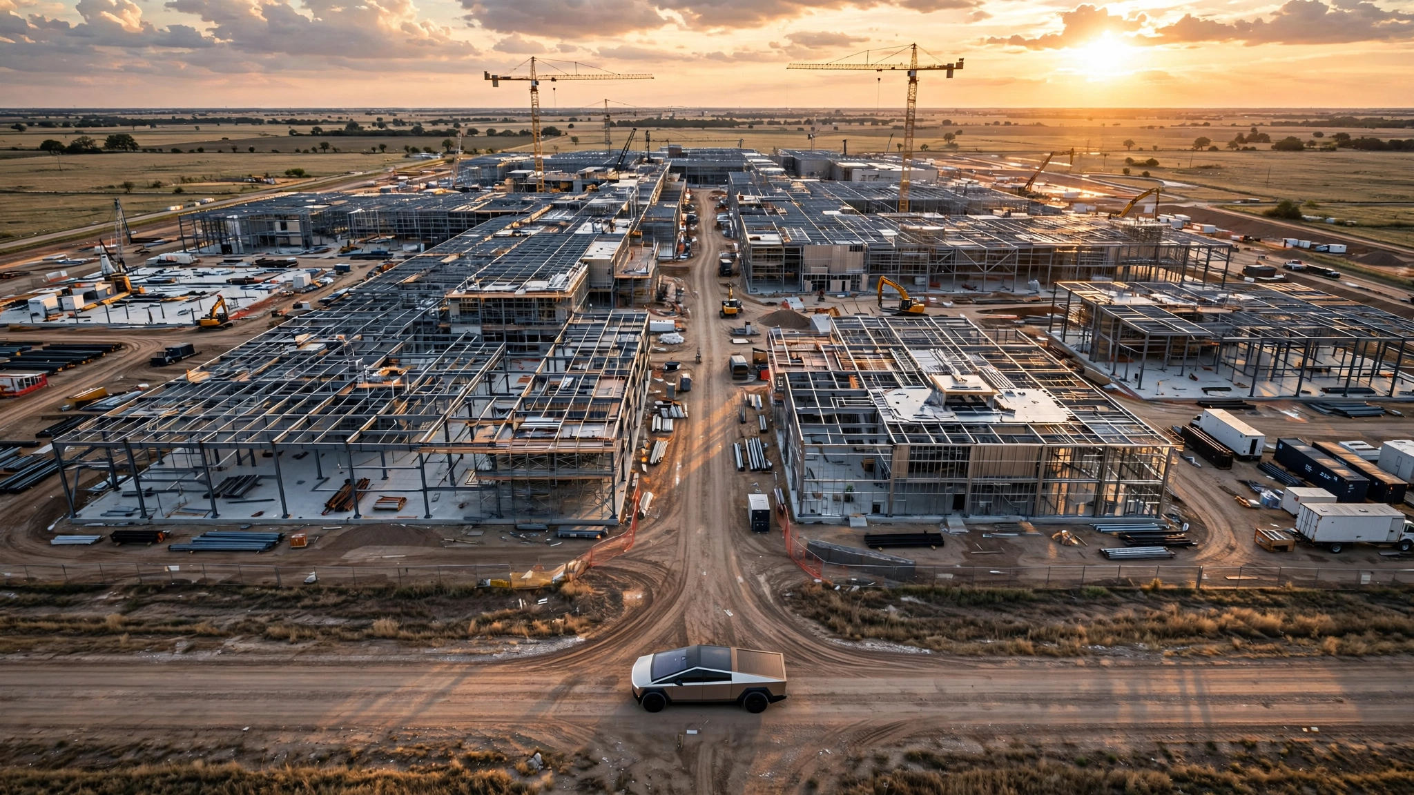
Fifty-five billion dollars. That is the initial investment SpaceX disclosed in its S-1 filing for Terafab, the semiconductor fabrication complex in Grimes County, Texas, that Elon Musk says will produce the chips powering Tesla's Optimus robots, Cybercab autonomous vehicles, and SpaceX's orbital data centers. Total investment across all phases could reach $119 billion, according to the same filing, which would make Terafab the single largest industrial capital commitment in American history outside of wartime mobilization.
Two data points arrived this week that suggest Musk is not bluffing. Tesla completed the tape-out of its AI5 chip, a design claiming 40× the performance of its predecessor, and sent it to Samsung and Taiwan Semiconductor for fabrication, with manufacturing ramp planned over the next 12 to 18 months. And Electrek identified Gary Jiang, a 17-year Intel veteran whose most recent role was managing Intel's 18A technology development transfer, tool installation, and ramp toward high-volume manufacturing, as Tesla's first named Terafab leadership hire. His LinkedIn title reads "Director, Tera Fab." He started this month.
Jiang's hiring is the clearest signal yet that Terafab is moving from presentation slides to personnel rosters. But hiring one fab director does not erase a fundamental question that nobody covering this story has bothered to answer with math: does the investment pencil out? Tesla has exactly one prior megaproject that attempted this kind of vertical integration at scale. It was called Battery Day, and it produced one of the most instructive execution trajectories in modern industrial history.
Battery Day: The Execution Coefficient
On September 22, 2020, Elon Musk stood on a stage at Tesla's Fremont factory and laid out a vision for 4680 battery cells that would, he said, deliver 10 gigawatt-hours of production within one year and 100 GWh by 2023, scaling eventually to 3 terawatt-hours by 2030. Maxwell Technologies' dry electrode process would cut manufacturing costs by 50 percent. Its structural battery pack would eliminate hundreds of parts. It was, in Musk's telling, the breakthrough that would make the $25,000 Tesla possible.
Five years and nine months later, this is what actually happened:
| Battery Day Promise | Target Date | Actual (June 2026) | Delivery % |
|---|---|---|---|
| 10 GWh production capacity | Sep 2021 | ~6 GWh (Giga Texas) | 60%, 4 years late |
| 100 GWh production capacity | 2023 | ~18 GWh (TX + Berlin combined) | 18%, 3+ years late |
| Dry electrode (both anode & cathode) | 2021 | Validated Q1 2026 | 5 years late |
| $25,000 Tesla enabled by cost reduction | ~2023 | Not shipped | 0% |
4680 production is not a failure. Tesla's in-house cells became its lowest-cost cell per kilowatt-hour by the end of 2024, beating what Panasonic and LG Energy Solution were charging. On both the anode and the cathode as of early 2026, the dry electrode process works, a genuine manufacturing breakthrough that no competitor has replicated at scale. Giga Berlin is expanding from 8 GWh to 18 GWh with a $250 million investment announced in May.
But the timeline slip is brutal, and the core manufacturing innovation needed six or seven complete revisions before it worked. Cybertruck, the primary vehicle for the cells, sells at a run rate of roughly 20,000 to 25,000 units per year against factory capacity for 250,000. South Korean cathode supplier L&F disclosed that its $2.9 billion materials contract with Tesla for 4680 production was written down to $7,386, a 99.97 percent reduction, citing a "change in supply quantity." At Battery Day in 2020, Musk said 100 GWh by 2023. Tesla has 18 percent of that target, delivered three years behind schedule, which produces what we might call the Tesla Execution Coefficient: the ratio of actual delivery to promised delivery at any given point.
That coefficient is not zero, and it is not hopeless, but it is 0.18.
The Wafer Math Nobody Has Run
Terafab will use Intel's 14A process node, a technology Intel confirmed in April when it joined the project as a manufacturing technology partner. Intel's 14A is comparable to TSMC's N2/A16 generation, the most advanced production node currently entering high-volume manufacturing anywhere in the world. To understand what it costs to build chips at this level, you need to understand what it costs to buy them from the only company that makes them well.
TSMC's wafer pricing is never officially disclosed, but industry estimates compiled by Tom's Hardware from multiple analyst sources reveal the trajectory:
| TSMC Node | Estimated Price/Wafer | Year Introduced |
|---|---|---|
| N5 (5nm) | $16,000 | 2020 |
| N3 (3nm) | $18,000–$20,000 | 2022 |
| N2 (2nm) | $30,000 | 2025 |
| A16 (1.6nm) | $45,000 (rumored) | 2026 H2 |
The relevant comparison for Intel 14A is the $30,000 to $45,000 range. Tesla and SpaceX currently buy their chips from Samsung and TSMC at these prices. Terafab's economic thesis is that making chips in-house will be cheaper than buying them at market rates.
Here is the calculation that tests that thesis, run at three utilization scenarios using SpaceX's own $55 billion Phase 1 investment figure and the 100,000 wafer starts per month target Musk described during Tesla's earnings call:
| Metric | Full Utilization (100%) | Moderate (70%) | Early-Stage (30%) |
|---|---|---|---|
| Wafer starts/month | 100,000 | 70,000 | 30,000 |
| Wafers/year | 1,200,000 | 840,000 | 360,000 |
| Capex amortized/wafer (15-yr life) | $3,056 | $4,365 | $10,185 |
| Est. opex/wafer (labor, chemicals, utilities) | $2,000 | $2,500 | $5,000 |
| All-in cost/wafer | $5,056 | $6,865 | $15,185 |
| Savings vs. $30K TSMC wafer | $24,944 | $23,135 | $14,815 |
| Annual savings | $29.9B | $19.4B | $5.3B |
| Capex payback period | 1.8 years | 2.8 years | 10.4 years |
At full utilization, the economics are extraordinary, and at 70 percent they still work. At 30 percent utilization, which is where most new fabs operate in their first two to three years, the payback period stretches past a decade and the per-wafer cost closes on TSMC's pricing, eliminating the rationale for building the fab at all.
This is the table that should be in every Terafab analysis and is not, because it reveals an uncomfortable truth: the investment thesis is entirely dependent on ramp speed. Every month of underutilization at a $55 billion facility costs roughly $306 million in idle depreciation. Apply the Battery Day Execution Coefficient of 0.18 to the 100,000 WSM target and you get 18,000 wafer starts per month, worse than the 30 percent scenario and deep in the territory where buying from TSMC would have been cheaper.
The Yield Question That Compounds Everything
The cost-per-wafer table above is generous. It assumes every wafer produces usable chips. In reality, leading-edge semiconductor manufacturing is defined by yields: the percentage of functional dies per wafer. TSMC's mature N3 process achieves yields of 70 to 80 percent. Its N2 process, still ramping, reportedly started below 60 percent. Intel's own recent track record is worse.
Intel's 10nm node, which the company rebranded as "Intel 7," took approximately five years from initial production to acceptable yields, a delay so severe that it cost Intel its manufacturing leadership and sent customers to TSMC. Intel's 18A process, the immediate predecessor to 14A, has documented yield challenges that industry analysts have tracked publicly. Jiang's hire is, in part, an acknowledgment that Tesla needs someone who has physically managed an 18A ramp to run Terafab precisely because yields at this node are not a solved problem even for the company that invented it.
For a brand-new fab operator with zero institutional semiconductor manufacturing experience, realistic first-year yields might be 20 to 30 percent. At a 25 percent yield, the effective cost per good die is four times the wafer cost, which means the $15,185 per wafer from the 30 percent utilization scenario becomes $60,740 per functional wafer equivalent. TSMC at $30,000 with 70 percent yields looks absurdly cheap by comparison.
The Strongest Case for Terafab
Everything above is true and also potentially irrelevant, for one reason: Tesla's 4680 program eventually worked. After six or seven revisions, the dry electrode process is now the company's lowest-cost cell technology. Its timeline was brutal, the ramp was slow, and the execution coefficient was 0.18. But the capability was built, and once built, it scales on a cost curve that external suppliers cannot match because the margin they charge for their expertise is gone.
Chipmaking at civilizational scale follows the same logic, and that is what Musk is actually planning. SpaceX's S-1 allocates 80 percent of Terafab output to D3 chips for orbital data centers and 20 percent to Tesla's AI5 and AI6 for autonomous vehicles and robots. Combined demand from the two companies, if Musk's product roadmaps are even half right, would consume hundreds of thousands of wafer starts per month indefinitely. At that scale, the 70 percent utilization threshold is not aspirational but inevitable, and the $55 billion investment amortizes into noise against the revenue it enables.
Battery Day's 4680 comparison also understates the learning advantage available for chip fabs. Tesla built its battery program from scratch. Terafab is being built on top of Intel's process technology, using Intel's equipment recipes, managed by Intel-trained engineers. Intel's formal partnership means Tesla is not inventing a process node but licensing one, which eliminates the most technically difficult part of semiconductor manufacturing and reduces the problem to operational execution.
TSMC CEO C.C. Wei's dismissive response when asked about Terafab may also be the wrong frame. "It takes two to three years to build a new fab, no shortcuts," he told reporters, and he is right about the timeline. But he is also right that TSMC cannot scale fast enough to meet the AI industry's demands, which is the entire reason Terafab exists. TSMC's own Arizona expansion is $100 billion for three fabs, operates at higher cost than Taiwan, and Lisa Su has confirmed these overseas facilities cost 5 to 20 percent more to operate. What matters here is not that Tesla will be better at making chips than TSMC. It is that TSMC cannot make enough chips.
Limitations
This analysis relies on estimated wafer pricing from analyst reports and industry sources, not TSMC's actual contract terms with Tesla or SpaceX, which are confidential. TSMC pricing is heavily volume-dependent, and Apple reportedly pays significantly less than standard rates. A benchmark of $30,000 per N2 wafer may overstate what a large customer like Tesla actually pays today.
Operating cost estimates use industry analogs for leading-edge fabs, not Terafab-specific projections, which do not exist publicly. Labor costs in Texas differ from those in Taiwan, Oregon, and Arizona, where comparable facilities operate. A 15-year depreciation schedule is standard for semiconductor equipment but may not reflect Terafab's actual accounting treatment, which SpaceX has not disclosed. As a descriptive ratio rather than a predictive model, the Battery Day Execution Coefficient has limitations; battery cell manufacturing and semiconductor fabrication are different disciplines with different failure modes, and the 0.18 coefficient may overstate or understate the difficulty of the chip fab problem.
The Bottom Line
Terafab is the most ambitious vertical integration bet in the semiconductor industry since Intel built its first captive fab in the 1980s, and it is being attempted by a company with exactly zero days of chip manufacturing experience. Its economics work beautifully at 70 percent utilization and catastrophically at 30 percent. Yield risk is real and unhedgeable without years of process engineering that Intel itself has not completed on the 14A node.
But Musk has a pattern that transcends any single project. He over-promises on timeline, under-delivers on schedule, and eventually builds the capability at a cost that retrospectively justifies the pain. At 18 percent of its target and five years late, the 4680 program hit its stride only after the dry electrode process it pioneered became Tesla's cost advantage. Apply the same pattern to Terafab and you get a chip fab that starts producing usable silicon around 2032 or 2033, roughly four years behind whatever Musk promises, at an initial cost overrun of 50 to 100 percent, and then slowly becomes the competitive moat Musk says it will be.
Every investor should be asking not whether Terafab will work. Given enough time and money, it probably will. What matters is whether $55 billion in idle capital during the ramp years would have earned more buying chips from TSMC and investing the difference in software, vehicles, and satellites. Tesla's Battery Day record says the first five years will burn cash at a rate that makes the current $55 billion estimate look optimistic, and SpaceX's own S-1 already hints at this: "There is no assurance [we] will meet Terafab objectives within expected timelines, or at all."
One final number. Tesla spent approximately $1.2 billion building its battery cell operation across Giga Texas and Giga Berlin, and it took five years to produce 18 GWh of capacity. Terafab Phase 1 costs 46 times more, the dry electrode process needed seven revisions, and leading-edge semiconductor fabrication involves more than a thousand discrete process steps compared to roughly two hundred for battery cell manufacturing. Every dimension of this project is harder and more expensive, and the only predictive baseline Tesla has says 18 percent delivery on the first timeline.
That is not a reason to bet against Musk. But it is a reason to bring a very large grain of salt.
What You Can Do
If you are an investor evaluating Tesla or SpaceX: build two models, one with Musk's timeline and one with a 4- to 5-year delay. Weight the delayed model at 80 percent, because the Battery Day track record is your base rate. Track the pace of senior fab hires from Intel, TSMC, and Samsung over the next 12 months; five or more Director-level-plus appointments would be a meaningful signal that Terafab is real infrastructure, not a recruiting exercise. Watch for Intel 14A yield data when it enters production in 2027; that number, more than any investment figure, will determine whether Terafab's economics work.
If you work in semiconductor manufacturing: Tesla is hiring aggressively for Terafab roles in Austin, specifically seeking people who have managed $100 million-plus capital expenditure projects and can oversee fab design from concept through execution. A talent war between Terafab and Intel's own operations will be one of the most consequential in the industry over the next two years.
If you just want to know when you will see a Tesla chip in a Tesla product: the AI5 is already taped out and at Samsung and TSMC for fabrication. You could be driving on a Tesla-designed chip within 18 months, well before Terafab produces a single wafer. Near-term product impact comes from chip design, not chip manufacturing, and the two should not be confused.