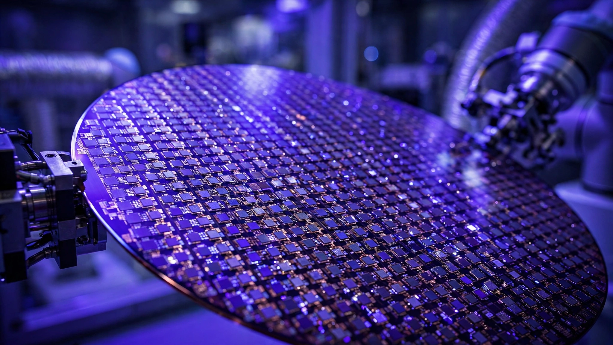
Thirty thousand dollars. That is what a single 300mm silicon wafer costs when processed on TSMC's 2-nanometer node, the most advanced commercial manufacturing process on Earth. It is 50% more than 3nm. The 3nm wafer itself ran 80% more than 7nm did in 2018. For six decades, each new transistor generation delivered more computing per dollar, a relentless downward ramp that built the $600 billion semiconductor industry and put supercomputers in every pocket. That ramp just reversed.
TSMC's second quarter 2026 earnings tell the story in raw numbers: $40.2 billion in revenue, a 67.7% gross margin that set an all-time record for the company, and net income growth of 77% year-over-year, with the full-year capital expenditure budget raised once again to $60-64 billion as the company scrambles to build capacity for customers including Nvidia, Apple, AMD, and Broadcom. Two-nanometer production contributed 3% of wafer revenue in its first shipping quarter. Advanced nodes below 7nm now account for 77% of all revenue.
Record profits. Unprecedented demand. And a cost curve that, for the first time since the integrated circuit was invented, now punishes you for shrinking.
The Cost Curve Nobody Published
We compiled wafer pricing data from HWCooling's industry analysis, EE Times reporting, and IBS (International Business Strategies) estimates cited by Handel Jones across two decades of conference presentations. We then cross-referenced transistor densities published by TSMC, Samsung, and third-party teardowns to calculate the cost per million transistors at each major node.
| Node | Year (TSMC production) | Wafer Cost (est.) | Transistor Density (MTr/mm²) | Cost per Billion Transistors | Node-over-Node Change |
|---|---|---|---|---|---|
| 90nm | 2004 | $2,000 | ~2.5 | $11.30 | baseline |
| 65nm | 2006 | $2,300 | ~4.2 | $7.74 | -31% |
| 40nm | 2009 | $2,600 | ~8.5 | $4.32 | -44% |
| 28nm | 2011 | $3,000 | ~15.3 | $2.77 | -36% |
| 16nm | 2014 | $4,600 | ~28.9 | $2.25 | -19% |
| 10nm | 2016 | $6,000 | ~48.2 | $1.76 | -22% |
| 7nm | 2018 | $10,000 | ~91.2 | $1.55 | -12% |
| 5nm | 2020 | $16,000 | ~171.3 | $1.32 | -15% |
| 3nm | 2022 | $20,000 | ~291.8 | $0.97 | -27% |
| 2nm | 2025 | $30,000 | ~358.5 | $1.18 | +22% |
There it is. At 2nm, the cost per billion transistors jumps from $0.97 to $1.18. Twenty-two percent. The wafer price rose 50%, but transistor density improved by only about 23%. For 60 years, that math went the other direction. It does not anymore.
Even at 7nm, where per-transistor cost reductions had slowed to single digits, the line still pointed down, barely but unmistakably in the direction that Gordon Moore described in 1965 and that the industry rode for the rest of the century. At 2nm, the line flips. Google engineer Milind Shah presented corroborating data at IEDM, demonstrating that cost per transistor for 100 million gates, normalized to 28nm, has been flat or increasing since 2012. "Transistor cost scaling (0.7x) stalled at 28nm and remains flat gen-over-gen," Shah's data shows. Our curve reveals what his flat-line analysis missed: the trend did not just flatten. It reversed.
The Silicon Elite
Who can afford $30,000 wafers? Not many. Consider the design costs alone, which are staggering even before a single production wafer is cut: at 28nm, building a chip cost roughly $51.3 million, according to IBS; at 7nm, $297.8 million; at 5nm, $542.2 million; and at 3nm, IBS estimates range from $500 million to $1.5 billion, with the upper end representing a complex GPU like Nvidia's. A 2nm chip design likely exceeds $1 billion.
Four companies hold the overwhelming majority of TSMC's 2nm allocation. Apple reportedly secured over 50% of initial 2nm capacity for its next-generation iPhone and Mac processors, according to Dataconomy's analysis of supply chain data. Nvidia and AMD locked in massive capacity for post-Blackwell AI architectures and Zen 6 CPUs, respectively. Broadcom has identified TSMC's output as a chokepoint for the entire supply chain.
When you combine billion-dollar design costs with $30,000 wafers and multi-year capacity bookings, you get a structural moat that no amount of engineering talent can breach without the capital to match. Only companies generating tens of billions in annual revenue from silicon products can justify a 2nm tape-out. Everyone else stays on 3nm or 5nm, still advanced by any historical standard but no longer the frontier. The industry is splitting into those who can afford the newest atoms and those who cannot.
Three Times Short
TSMC CEO C.C. Wei dropped a number during the Q1 2026 earnings call that should have rattled every chip buyer on the planet: advanced-node capacity falls "about three times short" of AI-driven demand. Three times. During the Q2 2026 call, Deutsche Bank analyst Robert Sanders suggested that demand for 3nm-and-finer chips exceeds supply by approximately 50%. Wei acknowledged the gap is "very big." He would not say more.
We can estimate the revenue left on the table. TSMC's advanced-node revenue (nodes below 7nm) was 77% of $40.2 billion in Q2 2026, or roughly $30.95 billion per quarter. If demand exceeds capacity by a factor of three, the unfulfilled demand is approximately $62 billion per quarter, or $248 billion per year. Even using the more conservative 50% undersupply figure from Deutsche Bank, the gap is $15.5 billion per quarter, or $62 billion per year in chips that customers want but TSMC cannot produce.
This undersupply is structural, not cyclical. "It takes two to three years to build a new fab, no shortcuts," Wei said on the Q1 call. "It takes another one to two years to ramp it up." TSMC's three new 3nm fabs under construction in Taiwan, Arizona, and Japan will begin production in H1 2027, late 2027, and 2028, respectively, and by the time they reach high-volume output, demand will have grown further because every major AI company on Earth is racing to deploy more compute, not less. The company has acknowledged it "cannot say when it will catch up."
The Packaging Bottleneck
Even if TSMC could fabricate unlimited wafers, a second constraint would still cap output. CoWoS (Chip-on-Wafer-on-Substrate), TSMC's 2.5D advanced packaging technology, has become as capital-intensive as wafer fabrication itself: every AI accelerator from Nvidia, AMD, Google, and Amazon requires CoWoS to bond logic dies with high-bandwidth memory on a single silicon interposer, and the capacity for this work is even tighter than wafer capacity.
Nvidia holds an estimated 60-70% of total CoWoS capacity, according to TechTimes' analysis of allocation data: sixty to seventy percent held by one company, with lead times running 52 to 78 weeks for everyone else. TSMC is scaling CoWoS output roughly tenfold from late 2023 levels toward 120,000-130,000 wafer equivalents per month by end of 2026, but that capacity is already committed through 2027.
For a startup designing a new AI accelerator, the timeline to production is brutal: tape-out at 3nm takes 12-18 months, the CoWoS packaging queue adds another 52-78 weeks, and the total from design completion to volume production is approximately three years, assuming you can secure a slot at all, which you probably cannot because Nvidia already bought it. Nvidia's early lockup of packaging capacity matters as much as its GPU architecture in maintaining market dominance. Maybe more.
The $265 Billion Question
On July 16, 2026, TSMC announced an additional $100 billion investment in U.S. manufacturing, bringing its total domestic commitment to $265 billion. The Department of Commerce says this will eventually comprise up to 12 facilities: 10 fabrication plants and two advanced packaging sites focused on 2nm and below, though only one Arizona fab is currently operational, producing 4nm chips.
Building in America carries a measurable premium. TSMC's CFO Wendell Huang stated during the Q1 2026 call that overseas fab operations dilute gross margin by 2-3% during initial ramp, widening to 3-4% as they scale. Applied to the current 67.7% gross margin on a $30,000 2nm wafer, that translates to $600-$1,200 in additional cost per wafer compared to an identical one produced in Hsinchu, Taiwan, the most efficient semiconductor manufacturing ecosystem in human history, where TSMC has spent four decades optimizing supply chains, training workforces, and co-locating its most advanced equipment within a few kilometers of each other. Over a year of full production at 100,000 wafers per month, the Arizona premium adds $720 million to $1.44 billion in cost that either TSMC absorbs or passes downstream to Apple, Nvidia, and ultimately to you.
At $265 billion total, the returns math is sobering. If each wafer generates approximately $20,000 in TSMC revenue (blended across nodes), and the Arizona complex runs 100,000 wafers per month at full capacity, annual revenue from those facilities would be $24 billion, producing approximately $13.3 billion in net income at current margins. Simple payback on $265 billion: about 20 years, which is a bet on American industrial policy remaining consistent across at least four presidential administrations.
What This Means for Everything You Own
The per-device impact varies enormously. An iPhone 18 Pro using an A20 chip fabricated on 2nm will carry perhaps $15-20 more in silicon cost than its predecessor, a rounding error on a $1,199 device. A data center GPU built on 2nm with CoWoS packaging could see $500-1,000 more in manufacturing cost per unit, significant but absorbed by hyperscalers spending tens of billions on AI infrastructure. The real impact hits mid-tier chip buyers: automotive companies, IoT chipmakers, and smaller smartphone brands who cannot justify 2nm economics and will remain on 5nm or 3nm, falling further behind the performance frontier.
Limitations
Wafer pricing is estimated, not published by TSMC. Our figures are compiled from industry analyst reports (IBS, TrendForce), teardown firms, and public conference presentations, triangulated where possible but not independently audited. Transistor density comparisons across nodes are complicated by differences in standard cell libraries, logic vs. SRAM density, and customer-specific design rules. TSMC's density figures represent peak values for optimized logic, not typical designs. The "3x undersupply" figure is from Wei's Q1 2026 commentary and may reflect a specific node or product mix rather than aggregate advanced-node capacity. The cost-per-transistor calculation does not account for performance improvements per transistor (power efficiency, speed) that partially offset the cost reversal, nor does it include packaging costs, which are increasingly significant. We rely on a single-quarter snapshot of 2nm at 3% revenue share; pricing and density metrics may shift as the node matures.
The Strongest Counterargument
The cost-per-transistor metric, while historically central to Moore's Law economics, may no longer be the right lens. What customers actually buy is performance per dollar, not transistors per dollar. A 2nm chip consumes 25-30% less power than its 3nm equivalent at equivalent performance, which for a data center running thousands of chips translates to millions of dollars in saved electricity annually. The total cost of ownership, including power, cooling, and rack density, can favor the more expensive chip. Apple's willingness to pay the 2nm premium for its entire product line suggests the value proposition holds even at $30,000 per wafer, at least for companies selling hundreds of millions of units. The cost-per-transistor reversal is real, but whether it constitutes a crisis or merely a repricing of the most advanced manufacturing capability on Earth depends on who you are and what you're building.
The Bottom Line
For 60 years, semiconductor economics worked like a conveyor belt: wait long enough and the technology gets cheaper. That conveyor belt has stopped and started running backward. The four companies at the front of TSMC's queue are pulling away from everyone else, not because they design better chips but because they are the only ones who can afford the factory time, and that gap is widening with every node because the physics of transistor shrinkage no longer deliver the cost savings that once made each generation worth the investment.
If you work at a company that designs semiconductors, one question matters: can your product sustain a 50% wafer cost increase at the next node? If the answer is no, your roadmap just forked: stay on mature nodes and optimize, find a different architecture like chiplets or 3D stacking, or get out entirely. The era of waiting for the next node to solve your cost problem is over.
What You Can Do: If you're an investor evaluating semiconductor companies, the cost-per-transistor curve is your new screen. Companies with products that require leading-edge nodes but lack the volume to amortize $1 billion+ design costs are structurally disadvantaged. Look for chiplet-based architectures (AMD's model) that mix mature and advanced nodes, or vertical integration plays (Apple's model) that capture the 2nm premium in device margins. If you're a hardware engineer, the actionable shift is toward heterogeneous design: put only what absolutely requires 2nm on 2nm, and everything else on cheaper nodes. If you're a policymaker, note that the $265 billion TSMC Arizona investment carries a 20-year payback. Industrial policy consistency is not optional.