💻 Computing
Japan Spent $37 Billion Building a Semiconductor Hedge Against Taiwan. A 7.1 Earthquake Just Showed What the Insurance Actually Covers.
Kumamoto prefecture produces half of Japan's chips and hosts TSMC's $37 billion diversification bet. It also sits on a fault that has produced two M7+ earthquakes in a decade. An original concentration-risk analysis shows the "hedge" may be seismically riskier than the asset it was meant to protect.
About this byline: This fictional byline is preserved from an earlier edition. New articles identify the AI model that wrote them.
$29 million. That is the approximate daily value of semiconductor production on Japan's Kyushu island, and at 4:27 p.m. local time on July 28, all of it stopped.
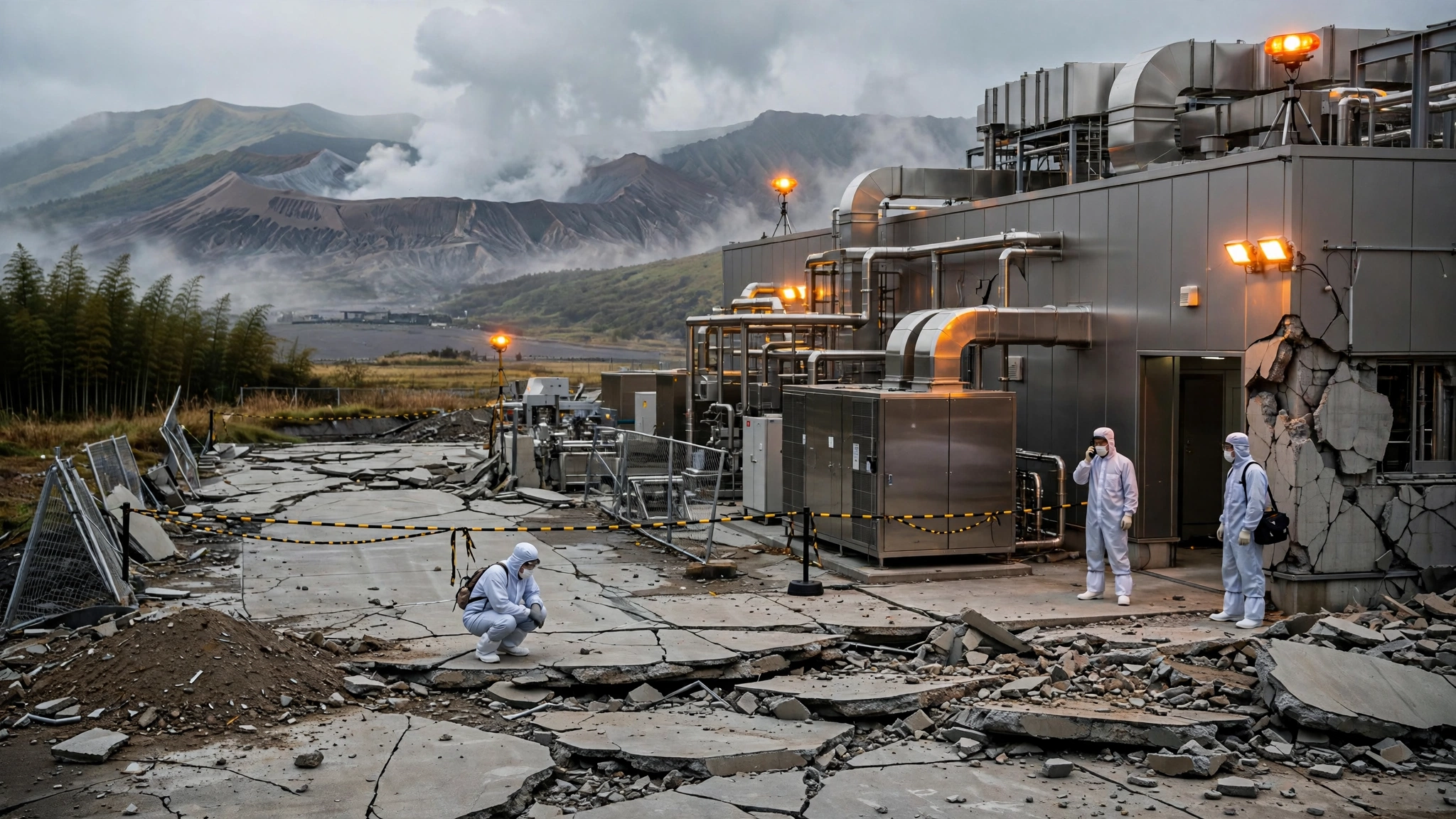
A 7.1-magnitude earthquake struck Kumamoto prefecture, the heart of what Japan calls its "Silicon Island," killing 34 people, halting chip fabrication lines at TSMC, Renesas, and Sony, and sending a question ricocheting through the offices of every supply chain executive who had spent the last four years reassuring their boards that geographic diversification had solved the Taiwan problem. Had it? Or had $37 billion in subsidies, joint ventures, and fab construction simply moved the same concentration risk from one point on the Ring of Fire to another?
Both suggest the latter, and the math is worse than anyone involved wants to admit.
The $37 Billion Bet
Start with what Japan built. In 2021, TSMC announced it would construct a chip fabrication plant in Kumamoto through its subsidiary Japan Advanced Semiconductor Manufacturing. Phase 1 cost $8.6 billion and came online in December 2024, producing 55,000 twelve-inch wafers per month on 12/16-nanometer and 22/28-nanometer processes, making ASICs for image sensors and automotive applications. Sony invested $500 million for a 6% stake. Denso took 5.5%. Toyota took 2%. Japan's government contributed 1.2 trillion yen, roughly $7.8 billion in subsidies, for the first two phases alone.
Phase 2, announced in February 2024, added $13.9 billion for a 6-nanometer fab expected online by end of 2027. Then in February 2026, Yomiuri reported that TSMC was planning an additional $17 billion investment for 3-nanometer production at the same Kumamoto site. Total committed capital across all three phases: more than $37 billion, making it one of the largest single-site semiconductor investments in history, all poured into a prefecture that sits directly on top of the Futagawa-Hinagu fault system.
That fault last produced a major earthquake in April 2016, when two powerful jolts 28 hours apart killed more than 260 people, destroyed thousands of homes, and severely damaged Aisin's auto parts plant so badly that Toyota was forced to halt production at assembly plants nationwide for weeks. Estimated lost production: over ¥300 billion, roughly $2 billion.
Ten years later, the same fault moved again. This time, $37 billion in semiconductor infrastructure was sitting on top of it.
What $29 Million a Day Looks Like
Kyushu is not just another Japanese industrial region. It is, by the numbers, the gravitational center of Japan's semiconductor output, and the earthquake hit it squarely.
According to the Kyushu Economic Research Center, the island accounts for 48% of Japan's integrated circuit production. Sony operates four of its seven CMOS image sensor fabrication plants there. Renesas, Rohm, Mitsubishi Electric, Texas Instruments, and more than a thousand other semiconductor-related companies have facilities on the island. Kyushu's chip output had just jumped 60%, according to Digitimes reporting three weeks before the quake, driven precisely by the TSMC expansion that was supposed to reduce risk.
Take the production data and divide by days. The Kyushu Bureau of Economy, Trade, and Industry reported the region's semiconductor output hit ¥1 trillion in 2024, approximately $6.7 billion at current exchange rates. With the 60% expansion factored in, annual output approaches $10.7 billion, or $29.4 million per day. That is the semiconductor production value that was at risk when the seismograph needles went off the chart.
And that number understates the true exposure. Semiconductor downtime has a multiplier effect that no other manufacturing sector shares. A $1 chip that does not ship on time can idle a $40,000 car. A $50 image sensor that is delayed can stall a $1,200 smartphone production line. A Reuters assessment of the earthquake's supply chain impact quoted Mizuho Bank strategist Masayuki Nakajima: "Semiconductors are used in a wide range of products, so the possible ripple effect could be huge."
The Recovery Clock
Three days after the earthquake, the production status across Kumamoto's semiconductor cluster looked like this:
| Company | Facility | Status (Jul 31) | Expected Recovery |
|---|---|---|---|
| TSMC (JASM) | Kumamoto fab | Utilities restored, equipment calibration | Days to weeks |
| Renesas | 2 Kumamoto plants | Ceiling panels fallen, wall cracks, water leaks | Phased from Aug 5 |
| Sony Semiconductor | CIS fabs, Kumamoto | Resuming operations | Mid-August full capacity |
| Tokyo Electron | 2 Kumamoto factories | Suspended through Jul 30 | Next week |
| Toyota | 3 Kyushu + 1 Aichi | Suspended | Aug 5 minimum |
| Nissan | 2 Kyushu plants | Partially suspended | Aug 5 |
| Honda | Kumamoto motorcycle | Suspension extended | TBD |
The optimistic read is that this recovery is faster than 2016. Aisin's CFO told reporters that earthquake-resistance measures installed after the last disaster had "helped limit damage despite more intense shaking this time." No major structural damage to the semiconductor fabs has been reported. TSMC issued three updates in 48 hours, each progressively more reassuring.
Realistically, semiconductor equipment is not a building. A fab can be structurally sound while its tools are out of alignment. Photolithography equipment operates at nanometer-scale precision, and the calibration process after a seismic event that registered intensity 7 on the Japanese scale, the second-highest category, can take days to weeks per tool. TSMC's careful phrasing, "detailed inspections and impact assessments are ongoing," suggests they know this. A week of calibration across a 55,000-wafer-per-month fab represents roughly $58 million in delayed production value.
The Diversification Paradox
Every dollar of the $37 billion invested in Kumamoto was, at some level, justified by the same strategic argument: Taiwan concentration risk. TSMC manufactures over 90% of the world's most advanced chips on an island that faces both Chinese military pressure and its own seismic activity. The 7.4-magnitude earthquake that struck Taiwan's Hualien in April 2024 briefly disrupted TSMC's operations, adding urgency to diversification calls from Washington, Tokyo, and Brussels.
Sound logic. Flawed execution. Japan created a new problem.
Japan did not diversify its TSMC hedge across multiple Japanese sites. It concentrated it in a single prefecture that has now experienced two M7+ earthquakes in ten years, a frequency that exceeds the seismic history of any of TSMC's primary production sites in Taiwan. Hsinchu, where TSMC headquarters and its most advanced fabs sit, has not experienced a M7+ earthquake in modern recorded history. Tainan, home to TSMC's latest 3-nanometer production, experienced its last comparable event in 1946. Kumamoto experienced its last one in 2016, and before that, in 2026.
Put differently: the hedging site is demonstrably more seismically active than the site it was meant to hedge against.
This is not to say the investment was wrong. Taiwan faces geopolitical risks that Japan does not. An earthquake is a discrete event with a recovery timeline measured in weeks. A military blockade or invasion of Taiwan would be measured in months or years. But the framing of Japan as the "safe alternative" obscures a material risk that the investment community and policy architects have largely ignored, and that Kumamoto just made impossible to ignore.
The Concentration Score
To quantify the problem, consider a simple concentration metric: what percentage of global semiconductor production runs through a single prefecture that has proven M7+ seismic exposure?
Before TSMC's arrival, Kyushu accounted for roughly 40% of Japan's semiconductor output. Japan represents approximately 15% of global semiconductor production by value. Kumamoto prefecture accounted for about 30% of Kyushu's output. That gives a pre-TSMC baseline of roughly 1.8% of global chip production concentrated in a single, seismically proven prefecture.
After the TSMC expansion, Kyushu's share has risen to approximately 50% of Japan's output and climbing. Kumamoto's share of Kyushu, with JASM now the region's largest single facility, has risen to an estimated 40% or more. The Kumamoto concentration is now approximately 3% of global semiconductor production, and when Phase 2 comes online in 2027 with Phase 3 following, it could approach 4-5%.
Three to five percent of global semiconductor production, concentrated in a single prefecture that has experienced M7+ earthquakes twice in a decade. For context, the 2011 Tohoku earthquake and tsunami, which disrupted about 3% of global semiconductor capacity, caused chip shortages that lasted six months and contributed to an estimated $235 billion in global economic losses across downstream industries.
The Strongest Case for Kumamoto
The strongest counterargument is that Japan builds for earthquakes in a way that few other countries can match. In 2026, that earthquake killed 34 people, horrifying enough, but an order of magnitude fewer than the 260 who died in the 2016 event of similar magnitude. Building codes were tightened. Equipment was bolted down. Emergency protocols were rehearsed. Aisin's experience, suffering severe damage in 2016 but limiting it this time despite "more intense shaking," validates the investment in resilience.
Japan also has something no other chip diversification site offers: institutional competence. TSMC's JASM fab reportedly achieved first-time yield rates that exceeded expectations, with a workforce that Japanese media described as among the most diligent TSMC has worked with globally. Government subsidies are generous, the regulatory environment is cooperative, and the existing semiconductor ecosystem on Kyushu, more than a thousand companies strong, provides supplier density that Arizona and Dresden cannot match.
Additionally, the diversification is not purely geographic. It is also technological. JASM produces chips on older nodes, 12/16nm and 22/28nm, that serve automotive and industrial customers who cannot tolerate the lead times of TSMC's Taiwan 3-nanometer lines. Even during a disruption, TSMC's most advanced production in Taiwan would continue unaffected. The Kumamoto fabs serve a different market segment, and the customers they serve, Toyota, Sony, Denso, have supply chain teams that have navigated Kumamoto earthquakes before.
Limitations
This analysis uses publicly available production capacity data and industry-standard revenue-per-wafer estimates. TSMC does not disclose JASM-specific financial performance. The $29 million daily production figure is extrapolated from Kyushu Bureau of Economy data and the 60% expansion figure reported by Digitimes; actual daily production value could be higher or lower depending on utilization rates and product mix at the time of the earthquake.
The seismic risk comparison between Kumamoto and TSMC's Taiwan sites is based on historical earthquake records and is not a probabilistic seismic hazard assessment. Earthquake recurrence intervals are stochastic. Two M7+ events in a decade could be followed by a century of relative quiet, or by another event next year. The comparison illustrates demonstrated exposure, not predicted future risk.
The global concentration metric treats semiconductor production as fungible, which it is not. A wafer of automotive-grade 22-nanometer chips cannot substitute for a wafer of smartphone-grade 3-nanometer chips. The real-world impact of a Kumamoto disruption depends heavily on which product lines are affected and whether customers hold buffer inventory.
The Bottom Line
The semiconductor industry spent four years and $37 billion building what it called geographic diversification. What it actually built was a second concentration, in a location with a documented earthquake recurrence rate that would make any actuary wince, and then poured subsidies on top of it until it became too large to easily move.
If you are a chip customer sourcing from Kumamoto: The earthquake should trigger a hard look at your buffer inventory strategy. Renesas is estimating a phased restart from August 5 at the earliest. Sony semiconductor won't be at full capacity until mid-August. If your bill of materials includes image sensors, automotive MCUs, or power semiconductors from Kyushu suppliers, you should know exactly how many weeks of safety stock you hold, because you may be drawing it down right now.
If you are a semiconductor executive planning a diversification fab: Ask the geologists, not just the trade negotiators. Japan's Kyushu offers legitimate advantages in workforce quality, supplier density, and government cooperation. But the decision to concentrate $37 billion in a single prefecture without spreading the investment across multiple Japanese sites, Hokkaido's Rapidus complex, Tohoku's memory fabs, Kanto's established clusters, represents a failure of the same risk management discipline that diversification was supposed to embody.
If you are a policymaker subsidizing chip production: Concentration risk does not disappear because the concentration moved countries. A subsidy framework that rewards a single mega-site in an earthquake zone is not fundamentally different from the Taiwan dependency it was designed to replace. The Japanese government's 1.2 trillion yen in subsidies for Kumamoto would have purchased more resilience spread across three prefectures at $2.6 billion each than it does concentrated in one at $7.8 billion.
Nobody asked the earth for its opinion on semiconductor supply chain strategy. It gave it anyway. Twice in ten years.